
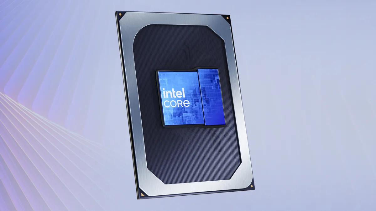
Intel is aggressively reshaping the entry-level computing market with its new Core Series 3 processors, codenamed Wildcat Lake. Detailed during a dedicated presentation at Hot Chips 2026, this budget-focused SoC skips legacy manufacturing nodes entirely, jumping straight from the Intel 7 process used in Raptor Lake-U to the cutting-edge Intel 18A process. Designed primarily for budget consumer laptops and edge devices, this architecture allows system vendors to build highly efficient machines without sacrificing modern connectivity.
The primary goal of the Wildcat Lake project was to deliver Intel's latest architecture to the budget market while strictly managing the bill of materials (BoM) and power targets. By leveraging a chiplet-based design, Intel provides a comprehensive toolset that covers the full spectrum of computing, from low-power edge deployments to massive data center servers like Diamond Rapids. This approach ensures that even entry-level users gain access to advanced platform technologies, including Wi-Fi 7 and Thunderbolt 4.
Architectural Cuts and Strategic Retentions
While Wildcat Lake is a distinct silicon design, it heavily reuses the architecture found in the premium Core Ultra Series 3 (Panther Lake). Intel retained the Panther Cove performance cores and Darkmont efficiency cores, alongside the Xe3 GPU architecture. However, to hit affordability targets, the engineering team had to make calculated reductions across the compute and I/O tiles.
To right-size the compute capabilities, Intel implemented several specific modifications:
- Reduced the overall number of P-cores and NPU engines.
- Integrated a smaller GPU and completely dropped hardware ray tracing support.
- Retained the XMX cores for AI workloads, despite initial plans to remove them.
- Removed a significant amount of cache and downsized the display controller, dropping support for DisplayPort UHBR capabilities.
- Eliminated camera PHYs entirely and reduced the number of PCIe lanes, saving approximately 15% in die area for the I/O chiplet compared to Panther Lake.
Despite these cuts, Intel preserved critical features that drive system efficiency. The dedicated power rails for the E-cores and the GPU remain intact, which is vital for maintaining battery life. Furthermore, the platform retains two Thunderbolt 4/USB4 heads and utilizes a narrower DRAM bus, directly reducing manufacturing costs for system vendors.
Ditching Foveros for UCIe and Organic Packaging
The most significant engineering pivot for Wildcat Lake is its packaging. Instead of using the complex and expensive Foveros technology, Intel opted for a two-die Multi-Chip Package (MCP) using standard organic packaging. To connect these chiplets, Intel utilized the Universal Chiplet Interconnect Express (UCIe) standard for the first time. While advanced packaging typically features a pitch of about 36 microns, this organic UCIe implementation uses a much wider 110-micron pitch.
This lower-density die-to-die connection perfectly reflects the reduced data bandwidth requirements of the chip. Because the display controllers do not support ultra-high bitrate modes, the interconnect does not need to handle massive data throughput. To maintain signal integrity and keep complexity low, Intel limited the link speed to 8 GT/sec. This decision kept the bit error rate low enough to avoid the need for complex retry and forward error correction techniques, even though it required a larger number of physical lanes.
Power management across the UCIe link was another major hurdle, especially since budget laptops often lack panel self-refresh technology. To meet strict battery life targets, Intel implemented buffers for the display links between the dies. This allows the links to drop into a low-power state and then burst data rapidly once the buffers are full.
Yield Recovery and Market Adoption
Manufacturing efficiency is critical for budget silicon, and Intel's die yield recovery strategy reflects this. The company developed multiple SKU configurations to utilize recovered chips effectively. Currently, about 29% of the compute dies are recoverable and usable within their active product stack, ensuring minimal silicon waste.
The market response has been overwhelmingly positive. Intel confirmed that Wildcat Lake has already secured over 70 design wins. The chip is now firmly positioned to replace the aging Raptor Lake-U series as the primary backbone of Intel's budget processor lineup.
The Blueprint for Affordable Silicon
The engineering choices behind Wildcat Lake signal a fundamental shift in how the semiconductor industry approaches budget hardware. Historically, entry-level chips were either monolithic dies built on older, depreciated nodes, or heavily defective high-end chips salvaged for lower tiers. By designing a bespoke, chiplet-based budget SoC on the bleeding-edge 18A process, Intel is proving that advanced manufacturing is no longer exclusive to flagship products.
The successful deployment of organic UCIe is the real breakthrough here. It demonstrates that chiplets can be economically viable for low-margin devices without requiring expensive Foveros packaging. If Intel can consistently packetize die-to-die communications efficiently over standard organic substrates, it paves the way for highly modular, ultra-cheap processors across the entire industry, effectively rendering the traditional monolithic budget CPU obsolete.
This article was written by AI from reporting by servethehome.com.