The semiconductor industry's long-running marketing illusion has finally hit a breaking point with the announcement of the IBM 0.7-nanometer chip. While the company claims this 7-angstrom technology is the most advanced in the world, the physical reality is that zero features on the silicon actually measure under one nanometer. This discrepancy has sparked sharp criticism from Elon Musk, who is now calling for a complete overhaul of how the tech world measures computing power.
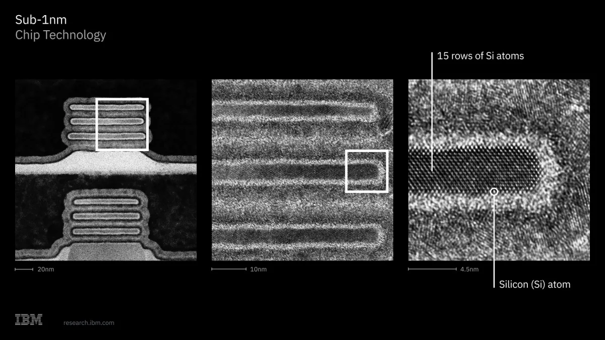
IBM's new process relies heavily on nanostacking, a method that vertically stacks transistors to drastically increase overall chip density. The development also utilizes advanced wafer bonding techniques to push performance boundaries. However, the company was unusually candid about the reality of its naming convention. In an official blog post, IBM admitted that the 7-angstrom label simply refers to a new generation of manufacturing, rather than the physical width of contacted metal wires as it did in past decades.
This admission caught the attention of Tesla and SpaceX CEO Elon Musk, who is currently driving his own Terafab project aimed at producing a terawatt of computing capacity annually. Responding to a user on X who called the sub-1 nanometer claim "highly misleading," Musk strongly agreed.
True, we should switch to naming process nodes according to the number of atoms wide of the smallest feature size. That would be most accurate imo.
- Elon Musk, CEO, Tesla and SpaceX
The disconnect between node names and physical reality is not new. The naming game fractured completely in 2021 when Intel rebranded its 10-nanometer process to "Intel 7" and its 7-nanometer process to "Intel 4." This shift was a direct response to Taiwan's TSMC, which had successfully captured massive market share by producing advanced chips for AMD, NVIDIA, and Apple using highly aggressive node marketing.
The Reality Behind the IBM 0.7-nanometer Chip
Musk's critique of the IBM 0.7-nanometer chip highlights a fundamental flaw in how the tech industry sells progress to both consumers and investors. For years, foundries like TSMC and Intel have used shrinking nanometer figures as a proxy for innovation, even as the physical limits of silicon forced them to scale vertically rather than horizontally. By shifting the metric to an atomic count, the industry could restore technical transparency, though marketing departments will fiercely resist losing their favorite buzzword.
Furthermore, as AI hardware demands push companies toward custom silicon and massive computing clusters - like Musk's own Terafab initiative - the actual density and power efficiency of a chip matter far more than its generational label. If a major player actually adopts an atom-based measurement standard, it could force a painful but necessary reset in semiconductor marketing, exposing which foundries are genuinely shrinking transistors and which are just shrinking numbers.