

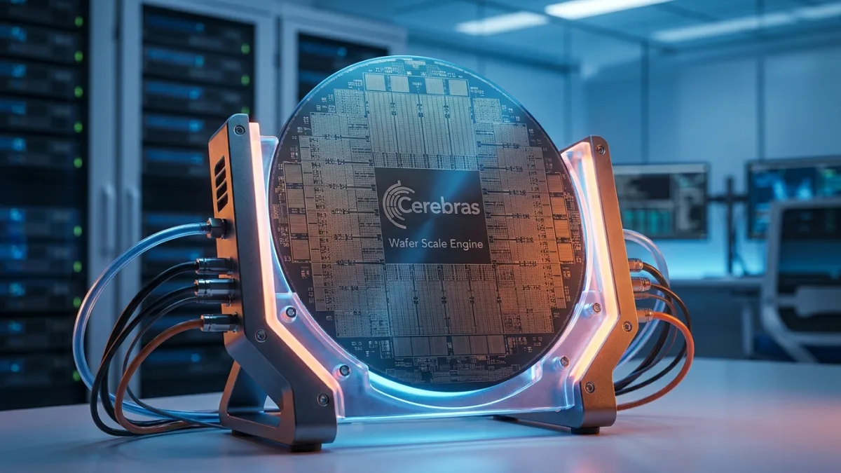
Cerebras Systems has unveiled the Cerebras Wafer Scale Engine, a massive artificial intelligence processor that shatters previous hardware limits by packing 1.2 trillion transistors onto a single silicon wafer. Measuring the size of a dinner plate, this breakthrough chip is 100 times larger than a standard processor and is engineered specifically to accelerate complex AI training workloads. While traditional computer chips are often smaller than a fingernail, Cerebras opted for wafer-scale integration, keeping the entire silicon wafer intact rather than slicing it into individual components.
For AI researchers and data center operators, this massive leap in scale eliminates the traditional bottlenecks of moving data between thousands of smaller, separate chips. By keeping the compute cores physically connected on one surface, the architecture drastically reduces the time and energy required to train next-generation AI models. As noted in coverage by The New York Times regarding the evolution of AI hardware, specialized silicon is becoming the defining factor in artificial intelligence progress.
The technical specifications of the Wafer Scale Engine represent a historic leap over existing hardware:
- Unprecedented Scale: The chip is 56 times larger than the biggest graphics processing unit (GPU) ever manufactured.
- Massive Core Count: It features 400,000 individual cores designed to work together through an extensive high-bandwidth communication fabric.
- On-Chip Memory: The processor includes 18 GB of on-chip SRAM, delivering 3,000 times more on-chip memory than traditional GPUs.
- Data Transfer: The architecture provides 33,000 times more bandwidth, utilizing tightly coupled memory for highly efficient data access.
The End of the Multi-Chip Bottleneck
The Cerebras Wafer Scale Engine represents a fundamental shift in how the industry approaches AI compute scaling. By keeping 400,000 cores on a single continuous piece of silicon, Cerebras bypasses the severe latency penalties incurred when data travels across motherboards between separate GPUs. In traditional supercomputers, moving data from one chip to another is the primary cause of slowdowns and power drain.
With 18 GB of on-chip SRAM, entire neural networks can theoretically be stored and trained directly on the processor without constantly fetching data from external memory banks. If this wafer-scale integration proves reliable in mass deployment, it could force established chipmakers to rethink their reliance on clustering thousands of smaller GPUs for heavy AI workloads. The sheer physical size of the chip presents unique cooling and manufacturing challenges, but the 33,000-fold increase in bandwidth offers a compelling reason to solve them.
This article was written by AI from reporting by kurzweilai.net.